F280049pzsr lqfp-100 single chip microcomputer (MCU / MPU / SOC) is the best price
explain
C2000 ™ The 32-bit microcontroller is optimized for processing, sensing and driving to improve the closed-loop performance of real-time control applications such as industrial motor drives, photovoltaic inverters and digital power supplies, electric vehicles and transportation, motor control, and sensing and signal processing.
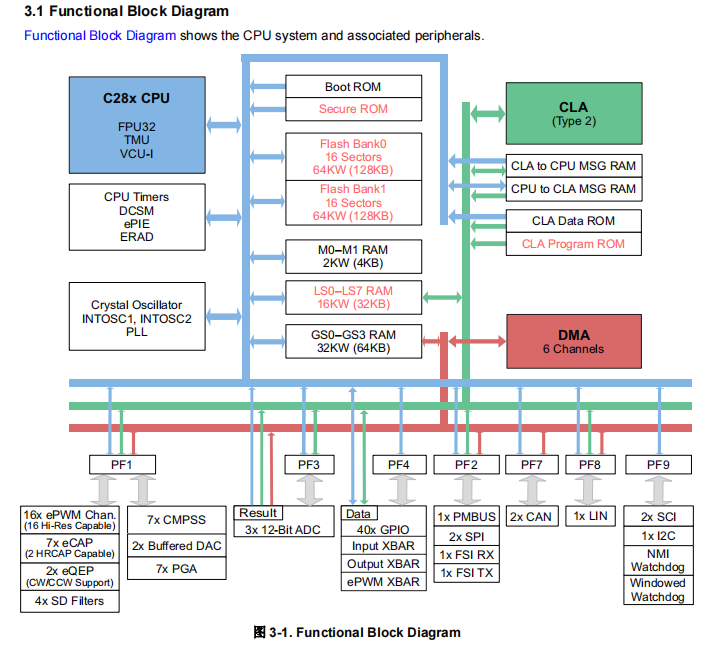
Tms320f28004x (f28004x) is a powerful 32-bit floating-point microcontroller unit (MCU), which allows designers to integrate key control peripherals, differential analog and non-volatile memory on a single device. The real-time control subsystem is based on TI's 32-bit c28x CPU and can provide 100MHz signal processing performance. The performance of c28x CPU has been further improved by the new TMU extended instruction set and vcu-i extended instruction set. The TMU extended instruction set can quickly execute the algorithm including common triangular operations in transformation and torque loop calculation. The vcu-i extended instruction set can reduce the delay of common complex mathematical operations in coding applications.
CLA allows a large number of common tasks to be unloaded from the c28x CPU. CLA is an independent 32-bit floating-point math accelerator that executes in parallel with the CPU. In addition, CLA has its own dedicated storage resources, which can directly access the main peripherals required in a typical control system. Like the main features such as hardware breakpoints and hardware task switching, ANSI C subset support is a standard configuration.
F28004x supports up to 256Kb (128KW) flash memory, which is divided into two 128KB (64KW) memory banks, supporting parallel programming and execution. In addition, up to 100kb (50KW) on-chip SRAM is provided in 4KB (2kW) and 16kb (8kw) blocks to achieve efficient system partition. It also supports flash ECC, SRAM ECC / parity and dual area security. The f28004x MCU integrates high-performance analog blocks to further support system integration. Three independent 12 bit ADCs can accurately and efficiently manage multiple analog signals, thus ultimately improving system throughput. The seven PGAs on the analog front end can realize on-chip voltage regulation before conversion. The seven analog comparator modules can continuously monitor the input voltage level for tripping conditions.
TMS320C2000 ™ The microcontroller includes advanced control peripherals (with epwm / hrpwm and ECAP independent of frequency), which can control the system excellently. The built-in 4-channel sdfm allows seamless integration of oversampling on the isolation layer Σ-Δ Modulator.
It supports connection through various industry common communication ports (such as SPI, SCI, I2C, Lin and can), and provides multiple multiplexing options to achieve excellent signal layout in various applications. The C2000 platform adds a pmbus that fully complies with the standard. In addition, FSI took the lead in realizing high-speed and reliable communication in the industry, supplementing the functions of various peripherals embedded in the device.
The specially implemented device model tms320f28004xc allows access to the configurable logic block (CLB) to realize additional connection functions, and also allows access to the secure ROM, which contains the ROM used to support instaspin-foc ™ Library for. For more information, see device comparison.
The embedded real-time analysis and diagnosis (ERAD) module enhances the debugging and system analysis functions of devices by providing additional hardware breakpoints and counters for analysis.
characteristic
• TMS320C28X 32-bit CPU
– 100MHz
– IEEE 754 single precision floating point unit (FPU)
– trigonometric mathematical unit (TMU)
• for common trigonometric functions and software libraries, from 3 × Cycle improvement
To 4 × cycle
• 13 cycle Parker transform
– Viterbi / complex math unit (vcu-i)
– ten hardware breakpoints (including ERAD) • programmable control law accelerator (CLA)
– 100MHz
– IEEE 754 single precision floating point instruction
– execute code independently of the main CPU
• on chip memory
– 256Kb (128KW) flash memory on two independent memory banks
Memory (ECC protection) – 100kb (50KW) RAM (ECC protection or parity protection
Protection) – support the dual zone security developed by the third party
– unique identification (uid) number • clock and system control
– two internal zero pin 10MHz oscillators
– on chip crystal oscillator and external clock input
– windowed watchdog timer module
– lost clock detection circuit
• 1.2V core, 3.3V I / O design
– internal vreg or DC / DC permissive capable of generating 1.2V
Single power supply design is allowed
– undervoltage reset (BOR) circuit
• system peripherals
– 6-channel direct memory access (DMA) controller
– 40 independent programmable multiplexed general purpose input / output (GPIO)
Pin
– provide 21 digital inputs on analog pins
– enhanced peripheral interrupt extension (epie) module
– support multiple low power consumption modes (LPM) with external wake-up function
– embedded real time analysis and diagnosis (ERAD)
• communication peripherals
– one power management bus (pmbus) interface
– an internal integrated circuit (I2C) interface
(pin bootable) – two can bus ports (pin bootable
Conducting) – two serial peripheral interface (SPI) ports
(pin bootable) – two serial communication interfaces (SCI) (pin bootable) – one local interconnect network (Lin)
– a fast serial interface (FSI) with transmitter and receiver
• analog system
– three 3.45msps 12 bit analog-to-digital converters (ADCs)
• up to 21 external channels
• each ADC has four integrated post-processing blocks (PPBS)
– seven digital analog with 12 bit reference
Window comparator (cmpss) of converter (DAC)
• digital interference filter
– two 12 bit buffered DAC outputs
– seven programmable gain amplifiers (PGA)
• programmable gain settings: 3, 6, 12, 24
• programmable output filtering
• enhanced control peripherals
– 16 with high resolution function (150ps resolution)
Epwm channel
• integrated dead band support with high resolution
• integrated hardware jump box area (TZ)
– seven enhanced capture (ECAP) modules
• high resolution capture (hrcap) on two modules
– two enhanced orthogonal codes supporting CW / CCW operation mode
Transmitter pulse (eqep) module
– four Σ-Δ Filter module (sdfm) input channel (each
Channel two parallel filters) • standard sdfm data filtering
• used in case of overestimation or underestimation
Fast operating comparator filter
• configurable logic block (CLB)
– enhance existing peripheral functions
– supports location manager solutions
• InstaSPIN-FOC ™ – Sensorless Field Oriented Control (FOC), using fast ™
Software encoder
– libraries in on-chip ROM memory
• package options: - 100 pin low profile Quad flatpack (LQFP)
[suffix PZ]
– 64 pin LQFP [suffix PM]
– 56 pin extremely thin leadless Quad flatpack (vqfn) [suffix
RSH]
• temperature options:
– s: – 40 ° C to 125 ° C junction temperature
– Q: temperature from – 40 ° C to 125 ° C under natural ventilation
Range
(approved by AEC Q100 for automotive applications)
application
• medium / short range radar
• air conditioning outdoor unit
• drive control of elevator door automatic opening and closing device
• automatic sorting equipment
• CNC control
• textile machine
• welding machine
• AC charging (pile) station
• DC charging (pile) station
• electric vehicle charging station power module
• vehicle wireless charging module
• energy storage power conversion system (PCS)
• central inverter
• solar power optimizer
• string inverter
• DC / DC converter
• inverter and motor control
• on board charger (OBC) and wireless charger
• AC drive control module
• AC drive power stage module
• linear motor power level
• servo driver control module
• AC input BLDC motor driver
• DC input (BLDC) motor driver
• industrial AC / DC power supply
• three phase UPS
• commercial network and server PSU
C2000 ™ The 32-bit microcontroller is optimized for processing, sensing and driving to improve the closed-loop performance of real-time control applications such as industrial motor drives, photovoltaic inverters and digital power supplies, electric vehicles and transportation, motor control, and sensing and signal processing.
Tms320f28004x (f28004x) is a powerful 32-bit floating-point microcontroller unit (MCU), which allows designers to integrate key control peripherals, differential analog and non-volatile memory on a single device. The real-time control subsystem is based on TI's 32-bit c28x CPU and can provide 100MHz signal processing performance. The performance of c28x CPU has been further improved by the new TMU extended instruction set and vcu-i extended instruction set. The TMU extended instruction set can quickly execute the algorithm including common triangular operations in transformation and torque loop calculation. The vcu-i extended instruction set can reduce the delay of common complex mathematical operations in coding applications.
CLA allows a large number of common tasks to be unloaded from the c28x CPU. CLA is an independent 32-bit floating-point math accelerator that executes in parallel with the CPU. In addition, CLA has its own dedicated storage resources, which can directly access the main peripherals required in a typical control system. Like the main features such as hardware breakpoints and hardware task switching, ANSI C subset support is a standard configuration.
F28004x supports up to 256Kb (128KW) flash memory, which is divided into two 128KB (64KW) memory banks, supporting parallel programming and execution. In addition, up to 100kb (50KW) on-chip SRAM is provided in 4KB (2kW) and 16kb (8kw) blocks to achieve efficient system partition. It also supports flash ECC, SRAM ECC / parity and dual area security. The f28004x MCU integrates high-performance analog blocks to further support system integration. Three independent 12 bit ADCs can accurately and efficiently manage multiple analog signals, thus ultimately improving system throughput. The seven PGAs on the analog front end can realize on-chip voltage regulation before conversion. The seven analog comparator modules can continuously monitor the input voltage level for tripping conditions.
TMS320C2000 ™ The microcontroller includes advanced control peripherals (with epwm / hrpwm and ECAP independent of frequency), which can control the system excellently. The built-in 4-channel sdfm allows seamless integration of oversampling on the isolation layer Σ-Δ Modulator.
It supports connection through various industry common communication ports (such as SPI, SCI, I2C, Lin and can), and provides multiple multiplexing options to achieve excellent signal layout in various applications. The C2000 platform adds a pmbus that fully complies with the standard. In addition, FSI took the lead in realizing high-speed and reliable communication in the industry, supplementing the functions of various peripherals embedded in the device.
The specially implemented device model tms320f28004xc allows access to the configurable logic block (CLB) to realize additional connection functions, and also allows access to the secure ROM, which contains the ROM used to support instaspin-foc ™ Library for. For more information, see device comparison.
The embedded real-time analysis and diagnosis (ERAD) module enhances the debugging and system analysis functions of devices by providing additional hardware breakpoints and counters for analysis.
characteristic
• TMS320C28X 32-bit CPU
– 100MHz
– IEEE 754 single precision floating point unit (FPU)
– trigonometric mathematical unit (TMU)
• for common trigonometric functions and software libraries, from 3 × Cycle improvement
To 4 × cycle
• 13 cycle Parker transform
– Viterbi / complex math unit (vcu-i)
– ten hardware breakpoints (including ERAD) • programmable control law accelerator (CLA)
– 100MHz
– IEEE 754 single precision floating point instruction
– execute code independently of the main CPU
• on chip memory
– 256Kb (128KW) flash memory on two independent memory banks
Memory (ECC protection) – 100kb (50KW) RAM (ECC protection or parity protection
Protection) – support the dual zone security developed by the third party
– unique identification (uid) number • clock and system control
– two internal zero pin 10MHz oscillators
– on chip crystal oscillator and external clock input
– windowed watchdog timer module
– lost clock detection circuit
• 1.2V core, 3.3V I / O design
– internal vreg or DC / DC permissive capable of generating 1.2V
Single power supply design is allowed
– undervoltage reset (BOR) circuit
• system peripherals
– 6-channel direct memory access (DMA) controller
– 40 independent programmable multiplexed general purpose input / output (GPIO)
Pin
– provide 21 digital inputs on analog pins
– enhanced peripheral interrupt extension (epie) module
– support multiple low power consumption modes (LPM) with external wake-up function
– embedded real time analysis and diagnosis (ERAD)
• communication peripherals
– one power management bus (pmbus) interface
– an internal integrated circuit (I2C) interface
(pin bootable) – two can bus ports (pin bootable
Conducting) – two serial peripheral interface (SPI) ports
(pin bootable) – two serial communication interfaces (SCI) (pin bootable) – one local interconnect network (Lin)
– a fast serial interface (FSI) with transmitter and receiver
• analog system
– three 3.45msps 12 bit analog-to-digital converters (ADCs)
• up to 21 external channels
• each ADC has four integrated post-processing blocks (PPBS)
– seven digital analog with 12 bit reference
Window comparator (cmpss) of converter (DAC)
• digital interference filter
– two 12 bit buffered DAC outputs
– seven programmable gain amplifiers (PGA)
• programmable gain settings: 3, 6, 12, 24
• programmable output filtering
• enhanced control peripherals
– 16 with high resolution function (150ps resolution)
Epwm channel
• integrated dead band support with high resolution
• integrated hardware jump box area (TZ)
– seven enhanced capture (ECAP) modules
• high resolution capture (hrcap) on two modules
– two enhanced orthogonal codes supporting CW / CCW operation mode
Transmitter pulse (eqep) module
– four Σ-Δ Filter module (sdfm) input channel (each
Channel two parallel filters) • standard sdfm data filtering
• used in case of overestimation or underestimation
Fast operating comparator filter
• configurable logic block (CLB)
– enhance existing peripheral functions
– supports location manager solutions
• InstaSPIN-FOC ™ – Sensorless Field Oriented Control (FOC), using fast ™
Software encoder
– libraries in on-chip ROM memory
• package options: - 100 pin low profile Quad flatpack (LQFP)
[suffix PZ]
– 64 pin LQFP [suffix PM]
– 56 pin extremely thin leadless Quad flatpack (vqfn) [suffix
RSH]
• temperature options:
– s: – 40 ° C to 125 ° C junction temperature
– Q: temperature from – 40 ° C to 125 ° C under natural ventilation
Range
(approved by AEC Q100 for automotive applications)
application
• medium / short range radar
• air conditioning outdoor unit
• drive control of elevator door automatic opening and closing device
• automatic sorting equipment
• CNC control
• textile machine
• welding machine
• AC charging (pile) station
• DC charging (pile) station
• electric vehicle charging station power module
• vehicle wireless charging module
• energy storage power conversion system (PCS)
• central inverter
• solar power optimizer
• string inverter
• DC / DC converter
• inverter and motor control
• on board charger (OBC) and wireless charger
• AC drive control module
• AC drive power stage module
• linear motor power level
• servo driver control module
• AC input BLDC motor driver
• DC input (BLDC) motor driver
• industrial AC / DC power supply
• three phase UPS
• commercial network and server PSU
• commercial communication power rectifier