XC2S30-5VQG100C Programmable Logic Device XILINX Original Stock
Overall Overview
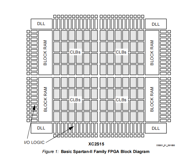
The Spartan II series FPGAs have a regular, flexible, and programmable configurable logic block (CLBs) architecture surrounded by a peripheral programmable input/output block (IOB). There are four delay locked loops (DLLs) in each corner of the mold. Two columns of block RAM are located on opposite sides of the mold, between the clb and IOB columns. These functional elements are interconnected through a powerful hierarchical structure of multifunctional routing channels
Spartan IIfpga is customized by loading configuration data into internal static memory units. With this method, unlimited Reprogramming cycles can be achieved. The values stored in these cells determine the logical functions and interconnections implemented in FPGA. Configuration data can be read from an external serial PROM (master serial mode), or written to the FPGA in slave serial, slave parallel, or Boundary scan mode.
Spardan II FPGA is typically used for high-capacity applications, where the versatility of fast programmable solutions adds benefits. Spardan II FPGA is an ideal choice for shortening product development cycles and providing a cost-effective solution for mass production.
Sparta iifpga achieves high-performance and low-cost operations through advanced architecture and semiconductor technology. Sparta ii devices provide a system clock rate of up to 200 MHz. In addition to the traditional advantages of high-capacity programmable logic solutions, Spardan-II FPGA also provides on-chip synchronous single port and dual port RAM (block and distributed forms), DLL clock drivers, programmable settings and resets on all triggers, fast logic portability, and many other functions.
Features
- Fully automatic mapping, placement, and routing