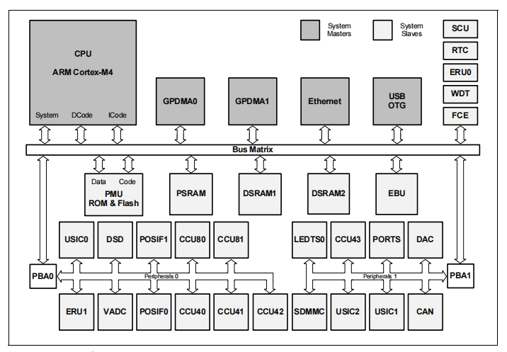
Figure 1 System Block Diagram
CPU Subsystem
• CPU Core
– High Performance 32-bit ARM Cortex-M4 CPU
– 16-bit and 32-bit Thumb2 instruction set
– DSP/MAC instructions
– System timer (SysTick) for Operating System support
• Floating Point Unit
• Memory Protection Unit
• Nested Vectored Interrupt Controller
• Two General Purpose DMA with up-to 12 channels
• Event Request Unit (ERU) for programmable processing of external and internal
service requests
• Flexible CRC Engine (FCE) for multiple bit error detection
On-Chip Memories
• 16 KB on-chip boot ROM
• 64 KB on-chip high-speed program memory
• 64 KB on-chip high speed data memory
• 32 KB on-chip high-speed communication
• 1024 KB on-chip Flash Memory with 4 KB instruction cache
Communication Peripherals
• Ethernet MAC module capable of 10/100 Mbit/s transfer rates
• Universal Serial Bus, USB 2.0 host, Full-Speed OTG, with integrated PHY
• Controller Area Network interface (MultiCAN), Full-CAN/Basic-CAN with 3 nodes, 64
message objects (MO), data rate up to 1MBit/s
• Six Universal Serial Interface Channels (USIC),providing 6 serial channels, usable as
UART, double-SPI, quad-SPI, IIC, IIS and LIN interfaces
• LED and Touch-Sense Controller (LEDTS) for Human-Machine interface
• SD and Multi-Media Card interface (SDMMC) for data storage memory cards
• External Bus Interface Unit (EBU) enabling communication with external memories
and off-chip peripherals
Analog Frontend Peripherals
• Four Analog-Digital Converters (VADC) of 12-bit resolution, 8 channels each, with
input out-of-range comparators
• Delta Sigma Demodulator with four channels, digital input stage for A/D signal
conversion
• Digital-Analogue Converter (DAC) with two channels of 12-bit resolution
Industrial Control Peripherals
• Two Capture/Compare Units 8 (CCU8) for motor control and power conversion
• Four Capture/Compare Units 4 (CCU4) for use as general purpose timers
• Two Position Interfaces (POSIF) for servo motor positioning
• Window Watchdog Timer (WDT) for safety sensitive applications
• Die Temperature Sensor (DTS)
• Real Time Clock module with alarm support
• System Control Unit (SCU) for system configuration and control
Input/Output Lines
• Programmable port driver control module (PORTS)
• Individual bit addressability
• Tri-stated in input mode
• Push/pull or open drain output mode
• Boundary scan test support over JTAG interface
On-Chip Debug Support
• Full support for debug features: 8 breakpoints, CoreSight, trace
• Various interfaces: ARM-JTAG, SWD, single wire trace
1.1 Ordering Information
The ordering code for an Infineon microcontroller provides an exact reference to a
specific product. The code “XMC4<DDD>-<Z><PPP><T><FFFF>” identifies:
• <DDD> the derivatives function set
• <Z> the package variant
– E: LFBGA
– F: LQFP
– Q: VQFN
• <PPP> package pin count
• <T> the temperature range:
– F: -40°C to 85°C
– X: -40°C to 105°C
– K: -40°C to 125°C
• <FFFF> the Flash memory size.
For ordering codes for the XMC4500 please contact your sales representative or local
distributor.
This document describes several derivatives of the XMC4500 series, some descriptions
may not apply to a specific product.
For simplicity the term XMC4500 is used for all derivatives throughout this document.