UCC27614DR 8-SOIC gate drive IC TI original stock
describe
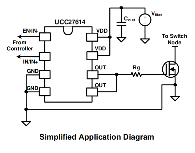
UCC27614 is a single channel, high-speed, low side gate driver that can effectively drive MOSFETs, IGBTs, silicon carbide, and gallium nitride power switches. UCC27614 has a typical peak driving strength of 10 A, reducing the number of ups and downs of power switches, reducing switch losses, and improving efficiency. The small propagation delay of UCC27614 equipment produces better power level efficiency by improving the Dead time optimization, pulse width utilization, control loop response and transient performance of the system.
UCC27614 can handle inputs of -10-V, which improves the robustness of medium ground bounce systems. The input is independent of the power supply voltage and can be connected to most controller outputs for maximum control flexibility. An independent enable signal allows the power stage to be controlled independently of the main control logic. If the system malfunctions (requiring the power transmission system to be shut down), the gate driver can quickly shut down the power stage. Enabling the function also improves the robustness of the system. Many high-frequency switching power supplies exhibit high-frequency noise at the gate of the power supply device, which can inject into the output pins of the gate driver, causing the driver to malfunction. UCC27614 performs well under these conditions due to its transient reverse current and reverse voltage capabilities.
If the VDD voltage is below the specified UVLO threshold, the strong internal pull-down MOSFET maintains low output. This active pull-down feature further improves the robustness of the system. The current driven by the 10-A of the UCC27614 device increases the system power density. This small package also provides optimal door driver placement and improved layout.
Features
• High power buffers