SN74AVC8T245DGVR buffer/driver/transceiver TI original stock
explain
This 8-bit cophase bus transceiver uses two independent configurable power rails. SN74AVC8T245 has been optimized to operate normally within the range of 1.4V to 3.6V for VCCA/VCCB settings. This device can operate normally when VCCA and VCCB are as low as 1.2V. Port A is designed to track VCCA. VCCA supports any power supply voltage within the range of 1.2V to 3.6V. Port B is designed to track VCCB. VCCB can accept any power supply voltage within the range of 1.2V to 3.6V, so it can perform universal low-voltage bidirectional conversion between voltage nodes of 1.2V, 1.5V, 1.8V, 2.5V, and 3.3V.
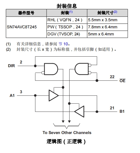
SN74AVC8T245 aims to achieve asynchronous communication between data buses. Based on the logic level on the direction control (DIR) input, this device sends data from the A bus to the B bus, or from the B bus to the A bus. Output Enable (OE) can be used to disable outputs, effectively isolating the bus.
SN74AVC8T245 is designed to power the control pins (DIR and OE) from VCCA.
SN74AVC8T245 is compatible with single power systems and can be replaced with '245' functionality in the future, with only a minor redesign of the printed circuit board.
This device fully complies with the specifications for partial power-off applications using Ioff. The Ioff circuit disabling the output prevents destructive current from flowing back from the device when it is powered off.
The VCC isolation feature ensures that as long as any VCC input is grounded (GND), both ports are in a high impedance state.
To place the device in a high impedance state during power on or off, the OE should be connected to the VCC through an pull-up resistor; The minimum value of the resistor is determined by the current injection capacity of the driver.
characteristic
The latch performance exceeds 100mA and meets the JESD 78 Class II specification
requirement
ESD protection performance exceeds the requirements of JESD 22 specification:
8000V human discharge model (A114-A)
-200V machine discharge model (A115-A)
1000V charger component model (C101)
Control input VIH/VIL levels based on VCCA voltage
VCC isolation characteristics - if any VCC input is grounded
(GND), then all I/O ports are in a high impedance state
Ioff supports local power outage mode operation
Fully configurable dual track design, supporting various ports from 1.4V to
Operating within the entire power supply voltage range of 3.6V
I/O can withstand a voltage of 4.6V
Maximum data rate:
-170Mbps (VCCA<1.8V or VCCB<1.8V)
-320Mbps (VCCA ≥ 1.8V and VCCB ≥ 1.8V)
application
Personal electronic products
• Industrial
• Enterprises
This 8-bit cophase bus transceiver uses two independent configurable power rails. SN74AVC8T245 has been optimized to operate normally within the range of 1.4V to 3.6V for VCCA/VCCB settings. This device can operate normally when VCCA and VCCB are as low as 1.2V. Port A is designed to track VCCA. VCCA supports any power supply voltage within the range of 1.2V to 3.6V. Port B is designed to track VCCB. VCCB can accept any power supply voltage within the range of 1.2V to 3.6V, so it can perform universal low-voltage bidirectional conversion between voltage nodes of 1.2V, 1.5V, 1.8V, 2.5V, and 3.3V.
SN74AVC8T245 aims to achieve asynchronous communication between data buses. Based on the logic level on the direction control (DIR) input, this device sends data from the A bus to the B bus, or from the B bus to the A bus. Output Enable (OE) can be used to disable outputs, effectively isolating the bus.
SN74AVC8T245 is designed to power the control pins (DIR and OE) from VCCA.
SN74AVC8T245 is compatible with single power systems and can be replaced with '245' functionality in the future, with only a minor redesign of the printed circuit board.
This device fully complies with the specifications for partial power-off applications using Ioff. The Ioff circuit disabling the output prevents destructive current from flowing back from the device when it is powered off.
The VCC isolation feature ensures that as long as any VCC input is grounded (GND), both ports are in a high impedance state.
To place the device in a high impedance state during power on or off, the OE should be connected to the VCC through an pull-up resistor; The minimum value of the resistor is determined by the current injection capacity of the driver.
characteristic
The latch performance exceeds 100mA and meets the JESD 78 Class II specification
requirement
ESD protection performance exceeds the requirements of JESD 22 specification:
8000V human discharge model (A114-A)
-200V machine discharge model (A115-A)
1000V charger component model (C101)
Control input VIH/VIL levels based on VCCA voltage
VCC isolation characteristics - if any VCC input is grounded
(GND), then all I/O ports are in a high impedance state
Ioff supports local power outage mode operation
Fully configurable dual track design, supporting various ports from 1.4V to
Operating within the entire power supply voltage range of 3.6V
I/O can withstand a voltage of 4.6V
Maximum data rate:
-170Mbps (VCCA<1.8V or VCCB<1.8V)
-320Mbps (VCCA ≥ 1.8V and VCCB ≥ 1.8V)
application
Personal electronic products
• Industrial
• Enterprises
Telecommunications